Field effect transistors are a switch device, in which current flows from a grounded Source terminal to a biased Drain terminal, due to voltage applied at Gate terminal; when the Gate voltage is removed, current stops flowing between Source and Drain. When such a device is made with organic semiconductors (OSC), which are molecular hydrocarbons or polymers, it is known as Organic Field Effect Transistors (OFETs). The charge carrier density of OSC is low, and hence the carriers are drawn from Source and Drain by Gate voltage to accumulate at the dielectric interface. The accumulated charge carrier sheet forms a conducting channel that enables current flow from grounded Source to biased Drain.
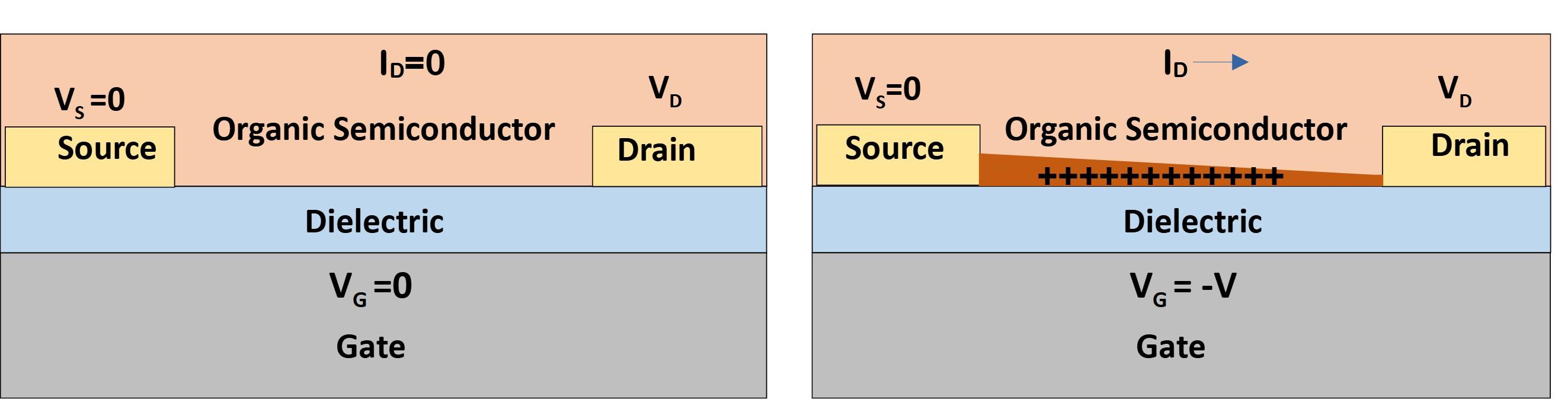
The OFET performance can thus be enhanced by increasing the charge carrier mobility of the OSC, which allows the charge carriers move at a higher velocity under electric field. Also, increasing the charge carrier density of the OSC would increase current by allowing more charge carriers to contribute to the current. Further, as charge injection from Source to OSC is essential for the current flow, any resistance at the interface of Source and OSC would serve to limit the device current. This is equivalent to an interface resistance being in series with resistance of channel, and hence value of this contact resistance must be significantly lower than that of channel.
The thesis shows three ways to improve the performance of OFETs.
- Molecular Structure: Two highly similar polymer semiconductors with an order of magnitude difference in charge carrier mobility presents an intriguing problem. Study of OFET characteristic combined with first principle calculations enables us to demonstrate that inclusion of rigid substituent group as the side chain pendant group significantly enhances the charge carrier mobility. ref.
- Self Assembled Monolayer at Electrodes: A remarkable increase in Threshold voltage and mobility, and decrease in contact resistance is brought about by functionalizing OFET electrodes with self assembled monolayer (SAM). However, the trends in device characteristics contradict the trends in work function, forcing us to rethink the mechanism of SAM. A combination of first principle calculations on the interface stack, and mathematical modeling of the interface energetics reveals the nature of energy level alignment at the interface and how the doping action of SAM increases charge carrier density in OSC.ref.
- Charge Transport in OFETs: A measurement of temperature dependent characteristics of the OFETs of different polymer OSC is carried out. The Arrhenius relationship between mobility and temperature is characterized by the activation energy and prefactor. Monte Carlo simulatios replicating the charge carrier path in OFET are carried out, varying the molecular as well as thinfilm properties in simulated grid. The simulation parameters leading to best match with temperature based characteristics exhibit the interplay between various factors governing charge transport and their relative effects. This enables us to point to charge transfer integral as the key parameter responsible for the evolution of charge transport properties of recent functional polymers.
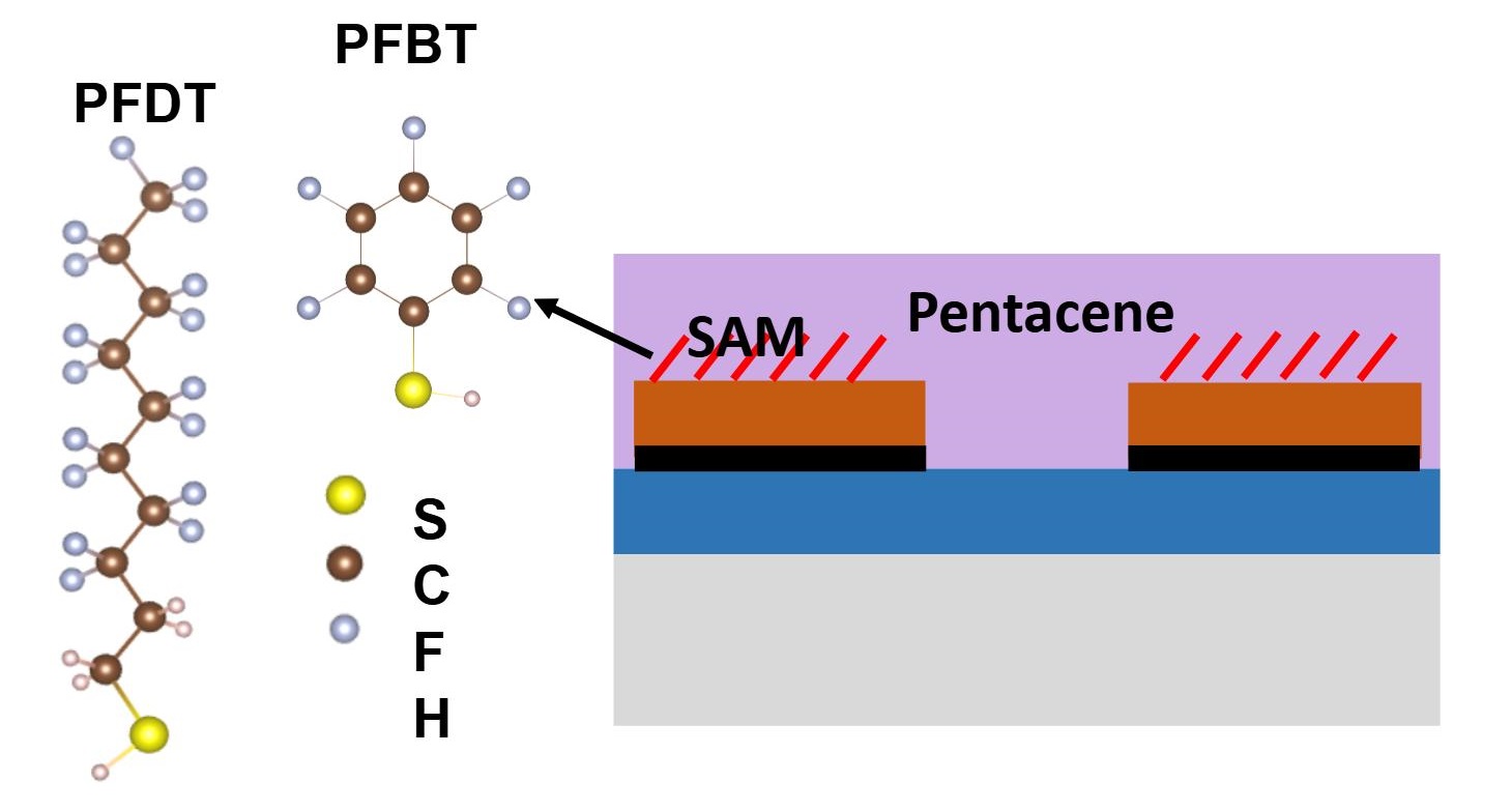
The interface of Source/Drain contacts with semiconductor has a resistance in series with the OFET channel. Being in series with the channel, if its resistance becomes higher than channel resistance, the device current will be low, no matter how efficient the channel is. One way to reduce resistance at interface is to insert a self assembled monolayer (SAM) of a polar material, which can reduce the energy barrier. But the exact mechanism of SAM is not established. We explored the action of SAM at electrodes by studying OFETs of pentacene having Cu electrodes functionalized by SAM of PFBT or PFDT molecules. The results enabled us to develop mathematical models to predict interface properties of SAM at electrodes, as well as device characteristics of SAM functionionalized OFETs. Ref.
Material & Device Characteristics
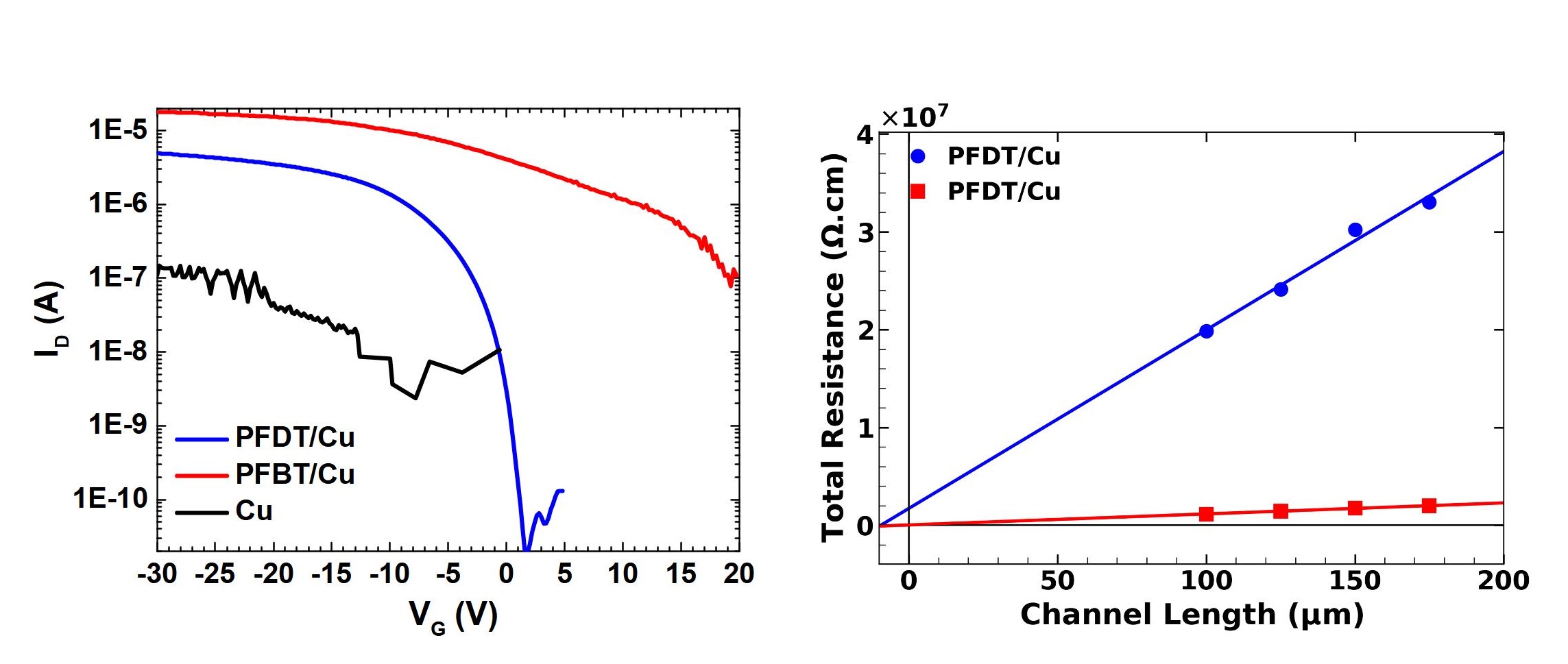
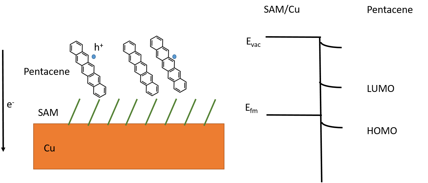
Layer of SAM on Copper increases its work function from -4.82 eV to -5.32 eV for PFBT and -5.54 eV for PFDT. Either is higher than the HOMO level of pentacene, and hole injection would be expected to improve. But the device characteristics tell another story. The current in PFBT devices is higher, its threshold voltage shifted to more positive values, and its contact resistance is lower than devices with PFDT. We seek to understand this contradiction in work function trends and device behaviour.
Interface Orbitals
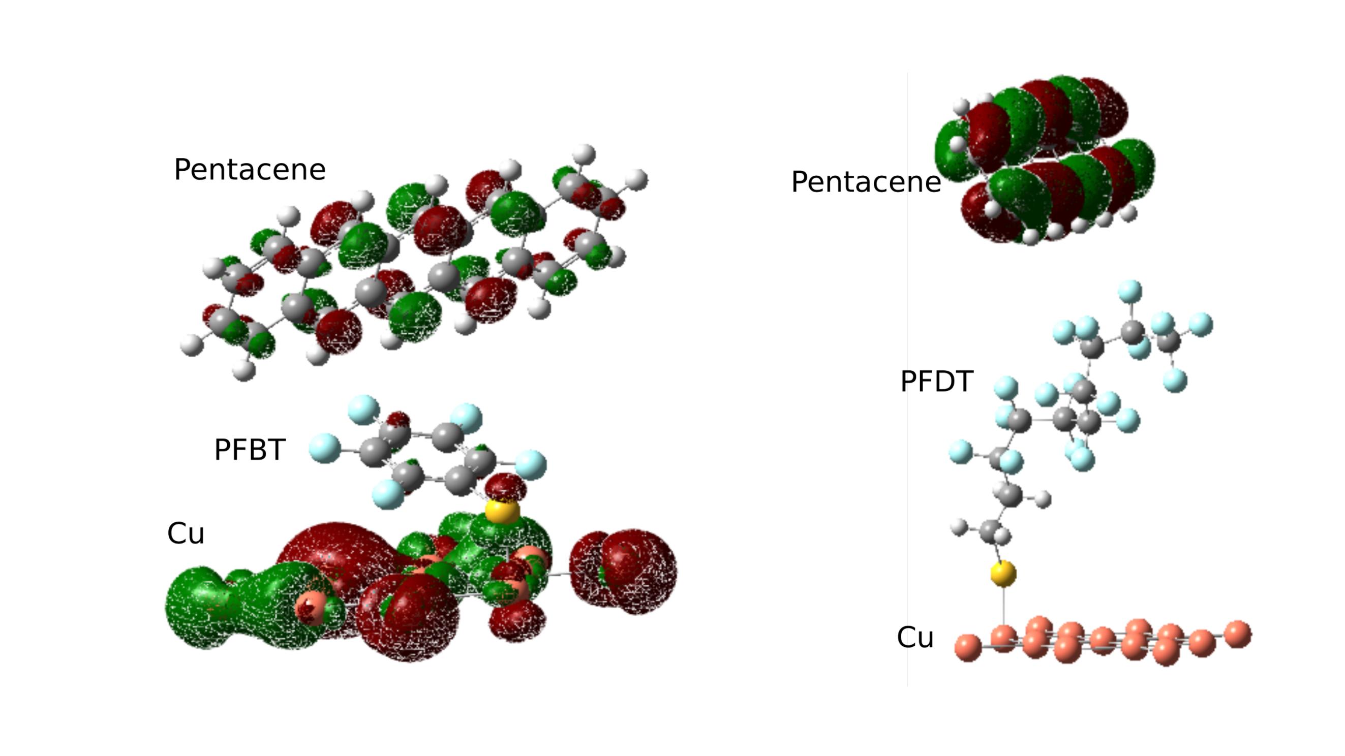
First principle calculations with the interface molecular configuration revealed a key difference between either SAM molecule at the interface. Calculations using density functional theory showed the HOMO of the Pentacene/SAM/Cu system for PFBT and PFDT. HOMO is located over the pentacene molecule in either case, but with PFBT it extends further to Cu electrodes. The delocalization of orbitals enables a faster charge transfer across this interface.
Mechanism of SAM at Electrodes
Combining device observations with ab-initio calculations allows us insight into the working of SAM at electrodes in OFETs. During interface formation itself, the energy levels of SAM/Cu tend to align at midgap of pentacene. This is achieved by electrons transferring from pentacene to SAM/Cu, leaving behind hole carrying pentacene cations, accompanied by bending of energy levels within pentacene. These excess holes increased conductivity of pentacene, allowing mobility to be higher and threshold voltage larger. The final alignment of energy levels is not at midgap, but rather the SAM/Cu level is pinned above the pentacene HOMO, with a mismatch which is the energy barrier.
Solving the Possion’s equation at the interface allowed us to calculate the charge carrier density and energy level bending within pentacene. The energy barrier at interface of pentacene and PFDT/Cu is higher than at PFBT/Cu, leading to the difference in contact resistance. The charge carrier density in pentacene in OFETs with PFBT/Cu is greater than with PFDT/Cu, explaining the difference in mobility and threshold voltage.
Device Model
The interface properties allows us to replicate the observed OFET characteristics. Knowing the excess charge carrier density in channel, we add the contribution to linear current by the excess charge carriers to that of accumulated charge carriers. As the device enters saturation regime, the pinch-off is delayed by the excess charge carriers which reduces Drain voltage to an effective channel voltage VC, and a gradual transition to Drain voltage independent Drain current occurs. The equations of OFET Drain current are modified for the conditions in SAM modified OFETs, and characteristics obtained.
$$ I_{D\mathrm{(Linear)}} = \left( qtn + C_i(V_G-V_T -V_D/2) \right) \mu V_D \frac{W}{L} $$ $$ I_{D\mathrm{(Presaturation)}} = \left( qtn + C_i(V_G-V_T -V_C/2) \right) \mu V_C \frac{W}{L} $$ $$ I_{D\mathrm{(Saturation)}} = \frac{\mu W}{2L} (V_G-V_T)^2 $$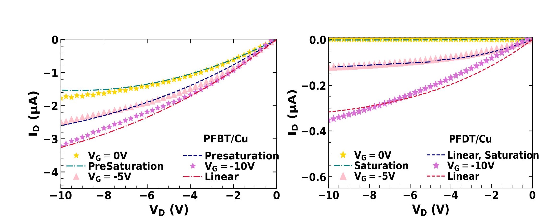
We have been able to establish that the alteration in energy level alignment and charge carrier doping of SAM/Cu influences the device characteristics.
Summary & Future Work
SAM functionalization has reduced contact resistance in OFETs to values comparable to the widely used Au electrodes, enabling the possibility of replacement. We demonstrated a novel mechanism of charge doping by SAM functinalised contacts. The analytical model developed to evaluate the extent of charge doping, and consequently device performance in SAM functionalized OFET, relied on measurment of a single device rather than multiple devices as required by TLM. DFT computations indicated the role of orbital delocalization in reducing contact resistance.
A computational model has now been developed predicting device performance on the basis of interface polarity and orbital delocalization. Ref.
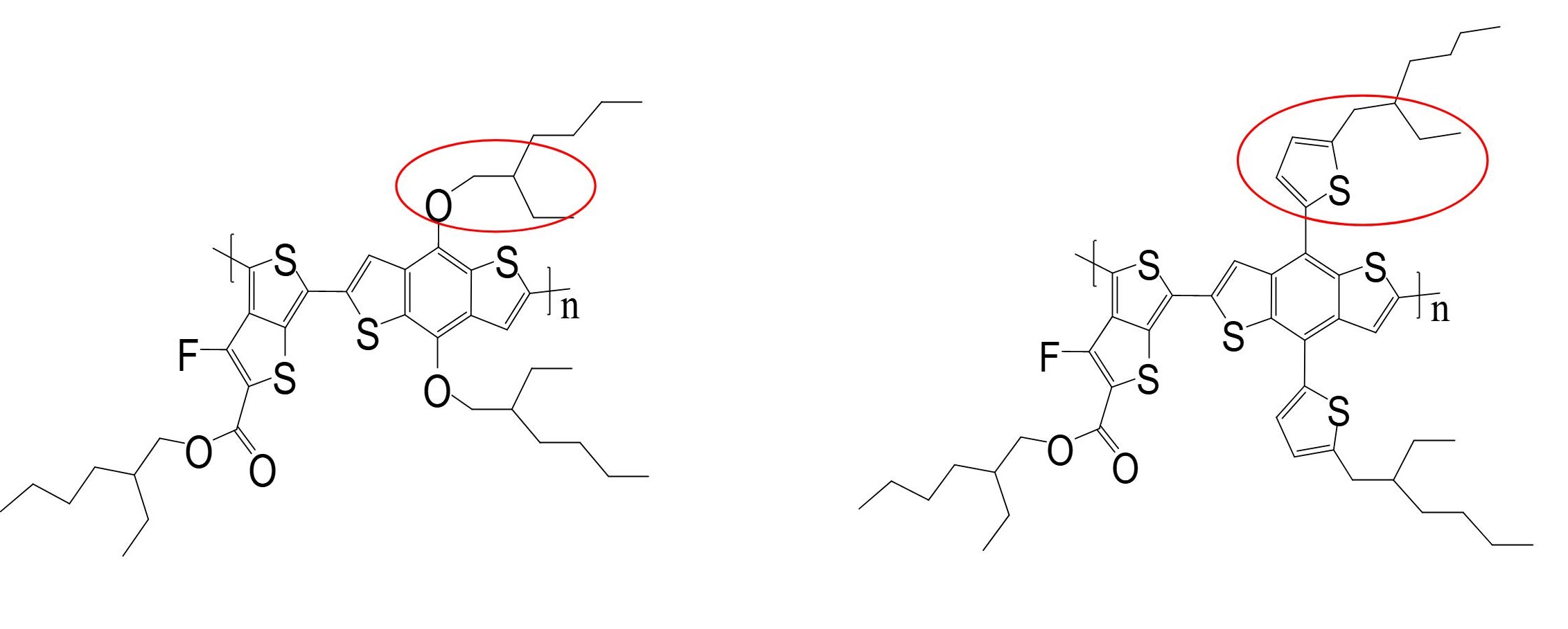
Varying the molecular structure or thinfilm morphology of polymers affect the charge transport in the films. But when two highly similar polymers are found to have highly different electronic properties, an investigation is called for. PTB7 and PTB7-Th are identical polymers, except the pendant group connecting side chains to main chain in PTB7 is an oxygen atom, while it is thiophene group in PTB7-Th. We found that their OFETs have order of magnitude difference in charge carrier mobility. First principle calculations on the respective polymer molecules reveal a vast difference in reorganisation energy brought about by changing the pendant group. This brings about a paradigm shift in the role of side chain substituent groups in affecting charge transport in polymers. Paper
OFET Characteristics
We fabricated OFETs with PTB7-Th and PTB7 as OSC. A bilayer dielectric was used to enhance the performance of OFETs. With this configuration, the Drain current of PTB7 devices was found to be an order of magnitude higher than previously reported. Further, this was the first report of OFETs with PTB7-Th. The FET mobility of PTB7-Th was found to be an order of magnitude higher than PTB7, which is unexpected for polymers identical in all aspects except side chain pendant group.

Charge Transfer in Molecules
To understand how subtle changes in molecular structure can bring about substantial changes in charge transport in the polymer, we look at the process of charge transfer between molecules. The transfer of charge is represented by the one electron Hamiltonian for polaron transfer, which considers the coupling of electron with the lattice, given as follows: $$ H = \sum_n \varepsilon_n a_n a^{\dagger}_n + \sum_{\lambda} h\omega_{\lambda} \left( b_{\lambda} b^{\dagger}_{\lambda} + \frac{1}{2} \right)\\ + \sum_{m,n} J_{mn} a_m a^{\dagger}_n \\ + \sum_{\lambda} \sum_n g^{2}_{n,\lambda} a_n a^{\dagger}_n \left( b_{\lambda} b^{\dagger}_{- \lambda} \right)\\ + \sum_{\lambda} \sum_{m,n} f^{2}_{m,n,\lambda} a_m a^{\dagger}_n \left( b_{\lambda} b^{\dagger}_{-\lambda} \right)\\ + \sum_n \delta \varepsilon_n a_n a^{\dagger}_n + \sum_{m,n} \delta J_{mn} a_m a^{\dagger}_n\\ $$ \( a^{\dagger}_n, a_n \) are respectively the creation and annihilation operator for an electron in an orbital of energy \( \varepsilon_n \) on site \( n \), and \( b^{\dagger}_{\lambda}, b_{\lambda} \) are the creation annihilation operators for a vibrational mode of energy \( h\omega_{\lambda} \). The first term is the total energy of the system. The second term describes charge transfer from site \( m \) to \( n \), where \( J_{mn} \) is the electronic coupling between sites \(n\) and \(m\). The third and fourth terms respectively consider the coupling of electronic levels with intramolecular vibrations, and intermolecular vibrations. \( g_{n,\lambda} , f_{m,n,\lambda}\) are the electron-phonon coupling for respectively intramolecular vibrations and intermolecular vibrations. \( \delta \varepsilon_n, \delta J_{mn}\) are respectively deviations in site energy due to static disorder, and deviations in electronic coupling due to dynamic disorder. Static disorder arises from spatial disorder that occurs in amorphous materials, due to the positions of sites being irregular. Dynamic disorder is the spatial disorder caused by vibration states of molecular sites. When \( \sum_{m,n} J_{mn} a_m a^{\dagger}_n\) exceeds the proceeding terms, electrons delocalize rapidly over electronically coupled sites and band-like transport occurs. In OSC however, as static and dynamic disorder significantly disrupt continuity in \( \varepsilon_n\) and \(J_{mn}\), electrons are localised on sites temporally before transferring to the next site. This process is known as hopping, as charges can be said to 'hop' from a localized site to next. Further, the electronic levels in molecular sites are strongly coupled to vibration levels, leading to the third and fourth term also having significant values.
Broadly, for charge transferring between molecules of a polymer, the dominant vibration levels are associated with the rearrangement of bonds within the molecule upon change in its charged state. When a neutral segment acquires a charge carrier from its neighbour, it undergoes changes in bond lengths and bond angles, as the additional charge disrupts the neutral configuration. The physical process of rearrangement consumes energy, known as Reorganization Energy (\( \lambda\)). Charge transfer occurs when the requirement of \( \lambda \) can be fulfilled. In other words, \( \lambda \) acts as an activation barrier to process of charge transfer. Further, charge transfer takes place only when the orbitals of the participating polymer segments overlap in space. The extent of overlap is represented by the parameter Charge Transfer Integral (J), which increases when the orbital area is high, and the orientation of molecules is more regular. This relationship between charge transport and the parameters reorganization energy and charge transfer integral are given by the Marcus equation, for rate (k) of charge transfer between identical molecules:
$$ k= \frac{J^2}{h} \sqrt {\frac{\pi}{\pi \lambda kT}} \exp\left({\frac{-\lambda}{4kT}}\right) $$Thus, charge transport is faster, and hence carrier mobility higher, with a lower (\ \lambda \), and a higher J.
Molecular Properties
To examine the effect of molecular properties and their effect on charge transport, we performed first principle calculations on the molecular structures as well as cations of PTB7 and PTB7-Th. Calculations were done by density functional theory (DFT) using package Gaussian09. Based on the difference of energy between ground state and cationic configuration for neutral or charged molecule, reorganisation energy was calculated for either monomer. From schematic shown below, reorganisation energy is calculated as:
$$ \lambda = E_0^0- E_0^+ +E_+^+ -E_+^0 $$
The RE of PTB7 is 340 meV, which is more than twice of the RE of PTB7-Th, 150 meV. Further, we assume that J is similar for both polymers, as their molecular structures are nearly identical, and it has been shown that the thinfilms of respective polymers also have highly similar morphology. With this assumption, based on the values of RE, Marcus equation shows that k is ten times higher for PTB7-Th than for PTB7.
Mobility Enhancement via Rigid Substituent Group
We found that PTB7-Th had an order of magnitude higher mobility as compared to PTB7 despite having nearly identical molecular structures and highly similar thinfilm morphology. The explanation for this was found by DFT calculations. The addition of the bulky thiophene group as the pendant group imparts rigidity to PTB7-Th and decreases the extent of rearrangement when charged. This reduces the RE of PTB7-Th to less than half of PTB7, and hence increases the mobility by an order of magnitude. We find that addition of a suitable substituent to reduce RE, which does not impact J, can raise the mobility of polymer significantly.
Summary & Future Work
OFETs fabricated with a PMMA-oxide bilayer dielectric enabled the fabrication of OFETs of polymers PTB7 and PTB7-Th having highest mobility reported. Mobility of OFETs of PTB7 and PTB7-Th was found to be an order of magnitude apart despite having identical conjugated structures. DFT computations revealed a significant difference in their reorganization energy, which analytical calculations confirmed to be corresponding to the difference in mobility. A rigid side chain group leading to a vast increase in mobility is a paradigm shift in the role of side chains in charge transport in polymers.
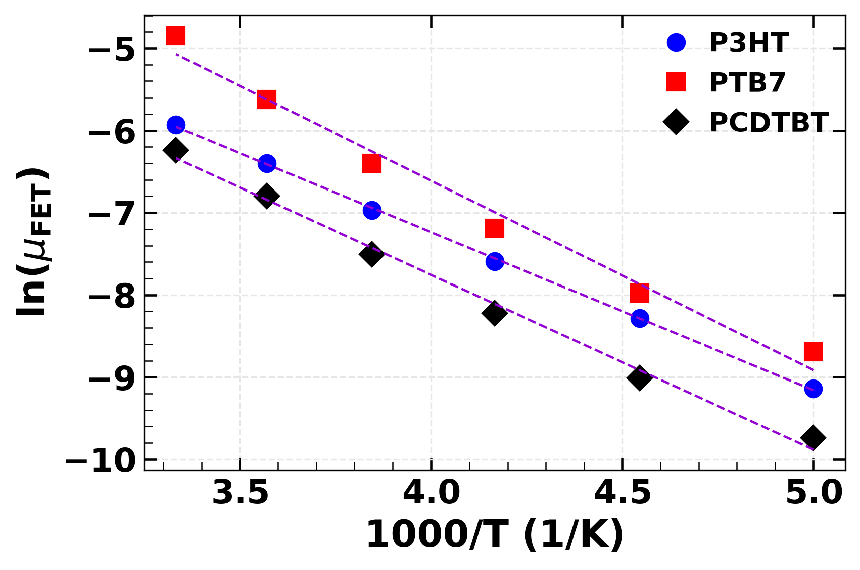
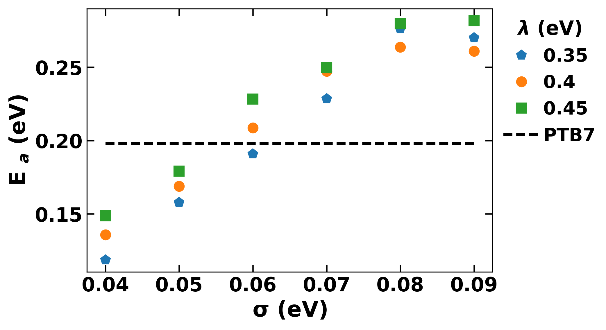
Charge transport in polymers occurs by hopping mechanism. Rate of transport depends on a number of factors such as properties of the molecule, morphology of the thinfilm, disorder within the thinfilm. Temperature dependent device characteristics reveal the details of charge transport in the material, but which of these parameters are actually behind them? A simulation replicating the devices at different temperatures presents a way to decouple these multiscale effects.
OFET Characteristics
We fabricated OFETs with P3HT, PCDTBT, and PTB7 as OSC. OFET charactristics were measured at low temperatures down to 200K, below which the device current was too low for consideration.
Simulations
A monte carlo based algorithm was developed to simulate charge transport in OFETs. Rate of charge transfer between neighbouring molecules was calculated based on Marcus equation, which determined the probability of hopping to that neighbour. A sequence of hops was performed to obtain mobility of charge carrier in the preset medium. Average mobility of several such sequences was taken to be the final value for that temperature.
Summary
We found the parameter space for different polymers which led to the experimentally observed device behaviour. The results clearly showed that high performing PTB7 was distinghuished due to its high charge transfer integral, rather than disorder as had been generally assumed.