Si quantum dot (QD) flash memories have several advantages including high fault toloerence and retentivity. The structure of these devices require arrays of Si QD grown on the dielectric film. SiO2 has been the dielectric of choice for Si based devices, due to the predictable and high performing nature of Si/SiO2 interface. However, the low dielectric constant of SiO2 himders scaling of its thickness. High-k dielectric such as HfO2 are alternatives enabling high capacitance and hence low thickness of the dielectric layer. However, interface of Si with HfO2 is not as highly optimized as with SiO2.
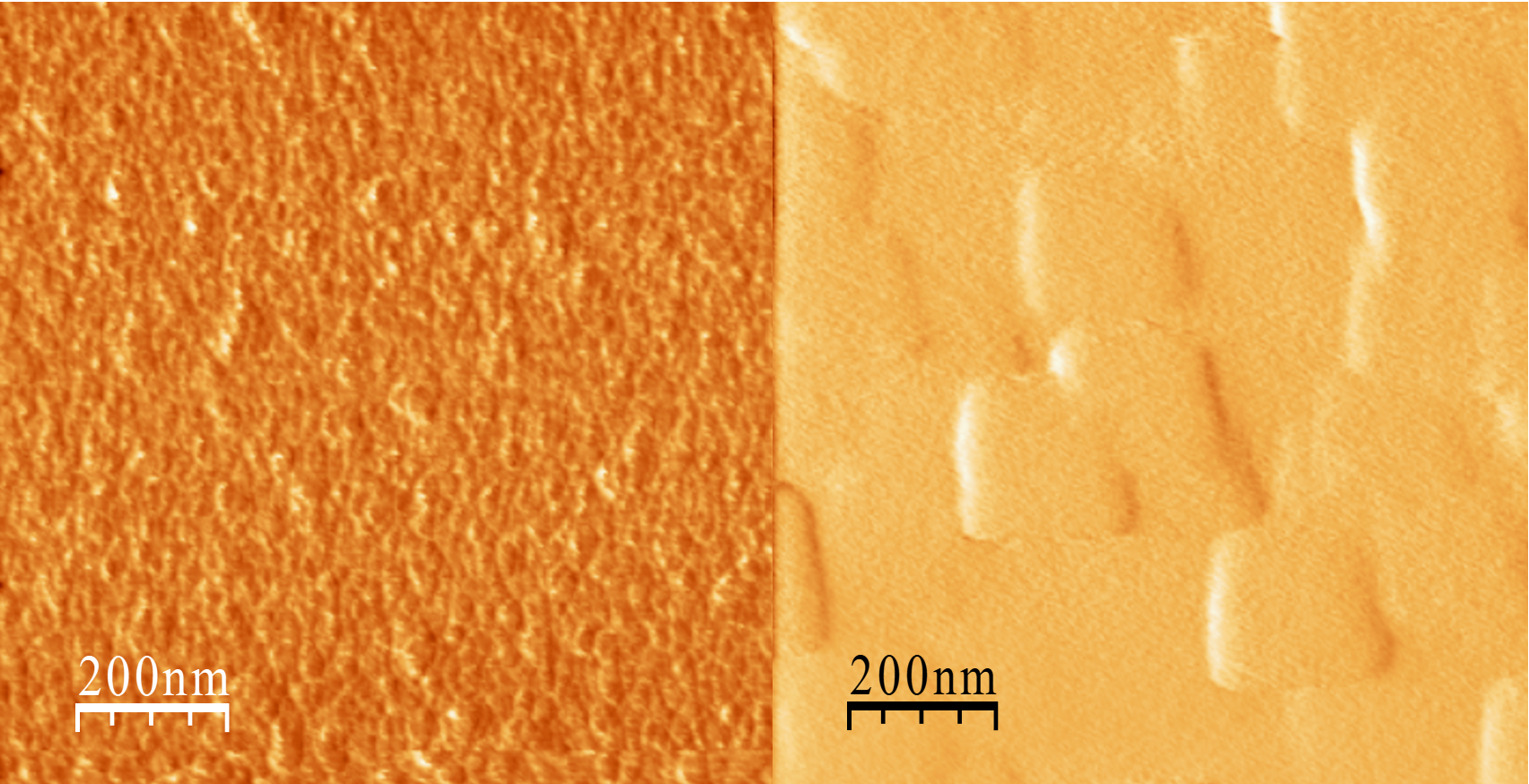
Here we explored the growth of Si QD on HfO2 by an approach of thermally stressing Si thinfilm. Density functional theory (DFT) based simulations confirmed the feasibility of formation of QD from thinfilm, due to the high thermal stability of Si QD-HfO2 interface. The thermal stability as obtained by DFT was found to be comparable to Si QD-SiO2 interface. To study the morphology and optimize the process for growth of Si QD on Hf2, following proceduere was carried out. HfO2 thinfilm was sputtered on Si wafer. Following this, amorphous or crystalline Si films were deposited on it by chemical vapour deposition, obtained by varying substrate temperature and vapour flow rate. Finally, the films were subjected to annealing, so as to stress the Si thinfilm into forming nanocrystals. As shown in the AFM image above, the annealing led to the formation of regular shaped nanocrystals from the coherent Si thinfilm. While QD were obtained from both crystalline and amorphous Si thinfilms, crystalline fiilms led to larger sized nanocrystals.
In this way, Si QD were grown on HfO2, as per the configuration required for scalable flash emmory devices.